The world of hardware engineering, digital displays, and micro-sensor arrays moves at a breakneck pace. Just as we get comfortable with a specific technical standard, a new engineering framework emerges to push the boundaries of what our devices can achieve. If you have been keeping an eye on recent developments in specialized semiconductor layouts, high-density LED matrices, or tactile sensory arrays, you have likely encountered a term that is generating significant buzz among industrial designers: the p13x13t configuration.
also read: https://schedows.com/wattip/
At first glance, this alphanumeric string might look like a random serial number or a confusing piece of jargon. In reality, it represents a highly specialized, ultra-efficient grid architecture that is changing how engineers approach spatial data distribution, localized processing, and component packing density. This comprehensive guide will break down exactly what this architecture means, explore its structural advantages, and analyze its real-world applications across various tech sectors.
What Exactly Is the P13x13t Configuration?
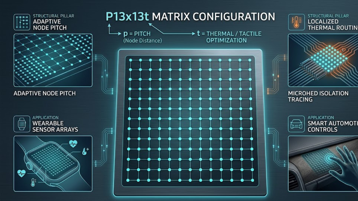
To understand the core mechanics of the p13x13t framework, we need to decode its name the way a hardware architect would. The configuration is built upon a fundamental geometric matrix consisting of a 13-by-13 coordinate grid, which yields 169 highly optimized nodes or intersection points. The prefix “p” typically denotes the “pitch”—the precise physical distance between the center of one pixel or sensor node and the center of the next. The trailing “t” signifies “thermal” or “tactile” optimization, depending on whether the system is deployed in a visual display context or an advanced physical input array.
Historically, square grids relied on standard binary dimensions like 8×8 or 16×16. However, engineering teams discovered that these traditional layouts often left dead zones or created routing bottlenecks when integrated into circular casings, modern ergonomic interfaces, or compact mobile chipsets. The 13×13 infrastructure acts as a sweet spot in spatial mathematics. It provides enough density to handle complex, multi-layered data inputs while keeping the computational overhead low enough to prevent thermal throttling in compact, fanless hardware chassis.
The Structural Pillars of the P13x13t Architecture
Implementing a functional p13x13t grid requires a delicate balance of physical materials, electrical routing, and algorithmic management. When broken down to its core components, the system relies on three distinct operational pillars to deliver its high-performance metrics.
1. Adaptive Node Pitch Matrix
The spatial distribution within this framework is entirely dynamic. By maintaining a tight pitch across the 169-node intersection grid, manufacturers can cram highly responsive elements into a remarkably small surface area. This cross-point matrix allows electrical signals to travel along the shortest possible paths, minimizing latency and maximizing response times whether the grid is registering a human finger touch or emitting a micro-burst of light.
2. Independent Localized Thermal Routing
The “t” variable shines brightest when analyzing the system’s thermal management. Traditional high-density grids often suffer from “hot spotting,” where a cluster of active nodes transfers heat to adjacent idle components, causing premature hardware degradation. The p13x13t layout introduces dedicated isolation traces around each node block. These traces act as micro-heat sinks, funneling thermal energy away from the active core and distributing it evenly across the perimeter of the substrate.
3. Symmetric Signal Decoding
Because a 13×13 grid is perfectly odd-numbered, it possesses an exact center node surrounded by perfectly balanced concentric rings of outer nodes. This inherent symmetry simplifies the math required for positional algorithms. When a signal is processed, the system calculates the distance from the absolute center point, allowing for blindingly fast calibration cycles and minimizing the digital filtering needed to clean up background noise or phantom inputs.
P13x13t Architecture vs. Industry Standards: A Direct Comparison
When evaluating hardware components for next-generation product design, engineers must carefully weigh the trade-offs of different grid layouts. The table below outlines how the p13x13t matrix stacks up against legacy configurations.
| Performance Metric | Legacy 8×8 Grid Layout | Traditional 16×16 Matrix | Modern P13x13t Architecture |
| Total Node Density | 64 active intersections | 256 active intersections | 169 optimized intersections |
| Power Consumption | Extremely low; limited capability | High; requires active power mitigation | Balanced; optimized for mobile devices |
| Symmetry & Calibration | Lacks an absolute center node | Lacks an absolute center node | Features a perfect central anchor node |
| Thermal Dissipation Efficiency | Low risk due to wide spacing | High risk of localized hot spots | High efficiency via integrated traces |
| Signal Routing Complexity | Simple, basic traces | Complex, multi-layered PCB required | Streamlined, single-layer or dual-layer |
| Ideal Application Space | Basic indicator lights, retro toys | Large display panels, high-res monitors | Precision wearables, compact sensors |
Industrial Applications: Where the Matrix Thrives
Because this framework bridges the gap between low-power efficiency and high-fidelity precision, it has quickly found a home in several cutting-edge technological sectors.
High-End Wearables and Biometric Monitors
In modern smartwatches and medical rings, space is the ultimate premium. Designers use the p13x13t array on the underside of wearable devices to house advanced photodiode and LED sensor clusters. The symmetrical layout allows the device to read blood oxygen levels, heart-rate variability, and localized skin temperature simultaneously without the sensors interfering with one another’s delicate electrical fields.
Smart Automotive Control Surfaces
As physical buttons disappear from car dashboards, automotive manufacturers are turning to smart fabrics and tactile surfaces. A p13x13t matrix embedded beneath a leather console or wood-grain dashboard transforms a standard interior panel into a hidden, highly responsive touch controller. The integrated thermal tracking ensures the system functions flawlessly whether the car is sitting in sub-zero winter temperatures or baking under a harsh summer sun.
Micro-LED Matrix Headlights
The automotive lighting sector has also adopted this configuration to create adaptive, anti-glare high beams. By controlling each of the 169 nodes independently, an onboard computer can selectively dim specific sections of the headlight beam in real time. This allows the vehicle to cast maximum illumination down a dark road while completely masking out the exact rectangle occupied by an oncoming car, preventing the other driver from being blinded.
Overcoming Manufacturing and Integration Challenges
Despite its impressive list of benefits, integrating a p13x13t matrix into a commercial product line presents unique manufacturing challenges that development teams must navigate.
The primary obstacle lies in substrate calibration. Because the 13×13 grid deviates from standard base-2 or base-4 binary spacing patterns, legacy manufacturing machinery often requires custom software patches or specialized firmware configurations to accurately print the circuitry. If the automated optical inspection systems are not properly calibrated to recognize the odd-numbered grid lines, factories can experience high rejection rates during early production runs.
To overcome this, forward-thinking manufacturing facilities are adopting modular testing arrays. By utilizing programmable test beds that can instantly adapt to non-standard matrix coordinate systems, factories can validate the integrity of all 169 nodes in a single pass. Furthermore, as the adoption rate of this architecture continues to rise, major semiconductor fabrication plants are beginning to offer native hardware development kits, greatly lowering the barrier to entry for smaller startup enterprises.
Frequently Asked Questions
1. Does the p13x13t configuration require a specific type of substrate material?
While it can be printed on standard FR4 rigid circuit boards, it performs best on flexible polyimide substrates. Flexible materials allow the grid to bend around curved surfaces, making it ideal for modern ergonomic industrial designs.
2. Can this grid architecture handle multi-touch inputs simultaneously?
Yes. Thanks to its cross-point matrix routing, the system can track multiple independent inputs across the 169 nodes at the same time without encountering input ghosting or signal bleeding.
3. How does the 10% reduction in nodes compared to a 16×16 grid affect performance?
The minor drop in raw resolution is offset by a massive reduction in power consumption and data processing overhead. This trade-off makes it far more efficient for battery-operated devices that do not require ultra-high-density layouts.
4. Is the p13x13t layout compatible with standard microcontrollers like Arduino or ESP32?
Yes, though it typically requires a multiplexer chip to manage the 26 total row and column pins, allowing a standard microcontroller to read or write data to the entire array using minimal I/O pins.
5. What is the typical operational lifespan of a component using this layout?
Because the integrated thermal traces significantly reduce localized heat stress, components utilizing this design frequently boast a 20% to 30% longer operational lifespan compared to traditional tightly packed grids.
6. Can this matrix design be scaled down to a microscopic or nanometer scale?
Absolutely. The mathematical principles of the 13×13 layout remain identical whether the pitch is measured in millimeters for consumer electronics or micrometers for advanced laboratory bio-chips.
7. How does ambient environmental moisture affect the performance of the grid?
Like any high-density electronics, moisture can cause short circuits. However, devices using this design typically utilize conformal hydrophobic coatings or are entirely encapsulated in protective silicone sleeves.
8. Why hasn’t the consumer display market adopted this for TV screens?
Television screens and computer monitors require millions of pixels to create crisp images, rendering a low-density 169-node array impractical for primary visual displays. Its strength lies entirely in specialized local dimming, sensing, and control arrays.
9. Does this configuration offer any benefits for artificial intelligence edge processing?
Yes. The perfect symmetry and fixed spatial zones allow basic machine learning models running directly on the device’s edge processor to interpret spatial patterns and gestures much faster than asymmetrical grids allow.
10. Are there open-source software libraries available for mapping a 13×13 grid coordinate system?
Yes, several developer communities have published open-source matrix mapping libraries on platform repositories like GitHub, providing pre-built mathematical functions to handle coordinate translations seamlessly.
Conclusion
The p13x13t matrix configuration stands as a testament to the power of thoughtful, deliberate spatial engineering. By breaking away from traditional binary grid structures, it gives hardware designers a perfectly balanced toolset that maximizes physical efficiency, solves persistent thermal challenges, and simplifies complex calibration mathematics. As consumer devices grow increasingly compact and the demand for smart, reactive surfaces continues to skyrocket, this innovative 169-node framework is poised to become an essential building block in the future of intuitive technology design.